YOUR BROWSER IS OUT-OF-DATE.
We have detected that you are using an outdated browser. Our service may not work properly for you. We recommend upgrading or switching to another browser.
Date: 19.05.2023 Category: general news, science/research/innovation

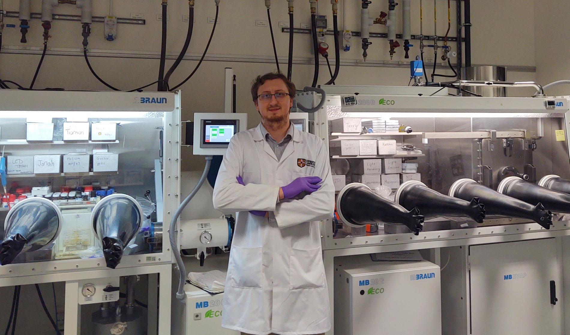
Szymon Zelewski, PhD, Eng. of the Faculty of Fundamental Problems of Technology has participated in the development of a high-brightness, high-performance LED whose light-emitting layer is made of a hybrid perovskite. The research results have been published in the prestigious journal Nature.

LEDs have conquered the market due to their efficiency, which far exceeds that of classic incandescent and fluorescent lamps. New materials are currently being explored globally that could increase LEDs’ functionality as well as reduce their production costs.
Such next-generation solutions, developed based on materials including organic semiconductors (OLEDs), consist of thin layers (less than 100 nm) and have thus been widely adopted in the displays of mobile devices such as phones and tablets. In the course of research into perovskite photovoltaics, it became apparent that perovskites could also be used, with minor modifications, in light-emitting diodes.
“This allows the development of competitive solutions that can be an alternative to even the best currently known solutions in terms of performance, chromaticity (colour purity), and the flexibility of the application process in industrial conditions,” explains Szymon Zelewski, PhD, Eng. from the FFPT.
The development of this technology was handled, as part of a project headed by Prof. Neil Greenham of the University of Cambridge, by several teams that belong to the Optoelectronics group at the Cavendish Laboratory. The group has led the way in the development of next-generation light-emitting diodes for many years. It is from here that the most cited papers in history on the subject of OLEDs, initiated and pursued to this day by Prof. Sir Richard Friend of the University of Cambridge, originated.
An international team, of which Szymon Zelewski, PhD, Eng. is a member, has developed a light-emitting diode (LED) characterised by high energy conversion efficiency and brightness, in which the light-emitting layer is made of a hybrid perovskite (formamidinium lead iodide, FAPbI3).
“Passivation of the material with an organic molecule (MSPE) increased its luminescence intensity by neutralising the material’s defects that adversely affect its properties while improving the transport of charge carriers (electrons and holes) between the perovskite layer and adjacent layers serving as electrodes,” says the W11 researcher.
This led to some of the best-ever parameters of diodes of this type, which is considered a significant achievement in the field of new energy conversion materials, which is notable – especially bearing in mind the current energy crisis.

As part of his tasks, Dr Zelewski performed optical measurements demonstrating the formation of additional energy states at the interface between electrode layers in the LED’s “sandwich” structure.
“They are a representation of the deteriorated current flow through the active layer of the diode and the emission of photons,” explains the researcher. “Instead, the injected charge carriers become trapped, causing energy loss in the form of heat, hence their name, which is ‘trap states’.
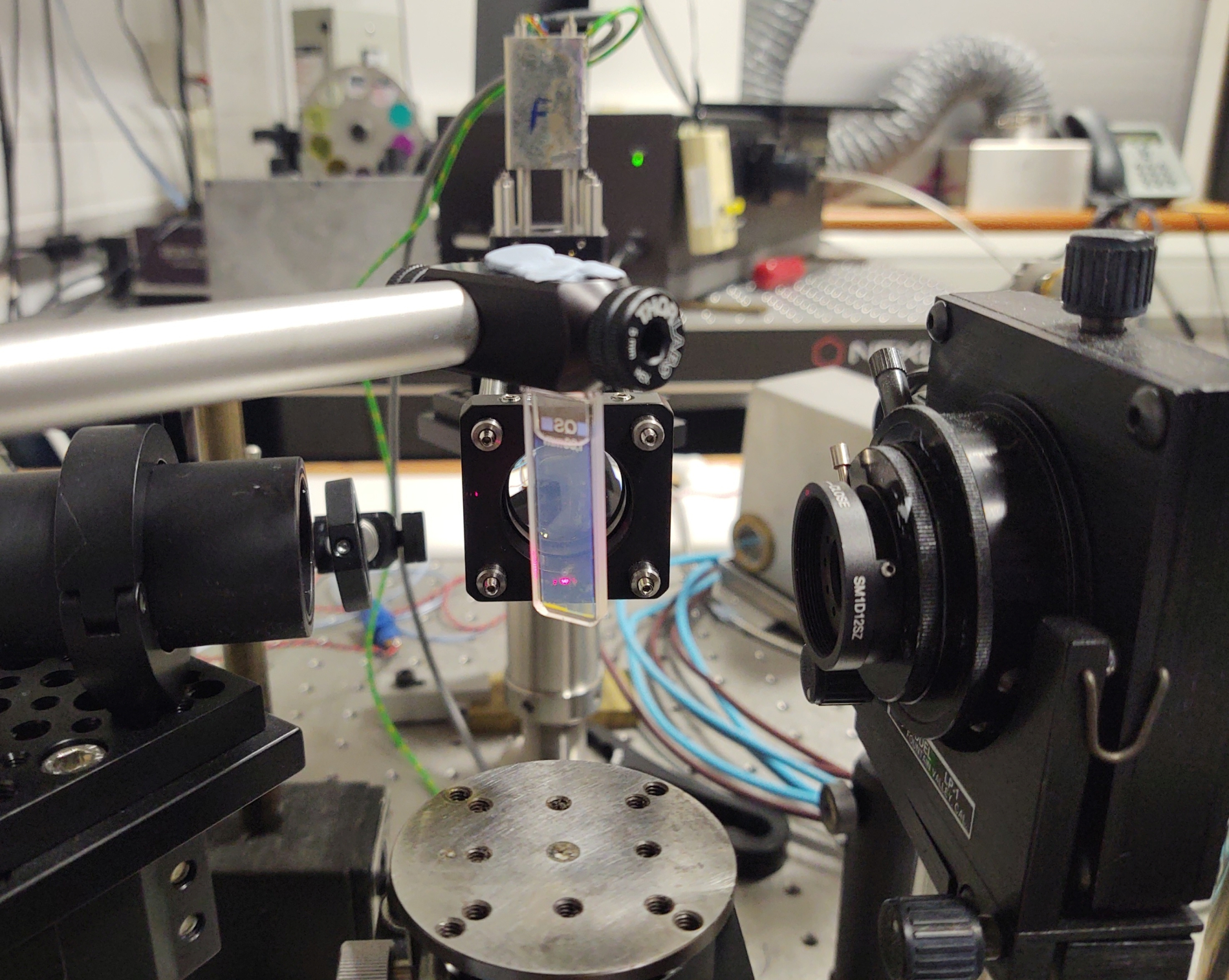
Their observation requires special experimental methods as they are relatively poor at absorbing light, which means that they are beyond the reach of classical spectrometers used in laboratories. Photothermal deflection spectroscopy (PDS) proved effective in this case. The method involves exciting a material with light and then detecting its temperature changes at the surface using a laser beam. Local heating of a special liquid changes its refractive index, leading to a change in the beam’s direction.
“I also developed a new procedure as part of the project works, allowing nanoparticles to be tested in a solution, from which a layer is produced to serve as a transparent electrode. This also made it possible to show the relationship between the structural disorder of the material and the performance of the diode, up until now commonly observed in photovoltaic cells.” – says Dr Szymon Zelewski.
Szymon Zelewski, PhD, Eng. has been at the University of Cambridge since 2021. To the. He is currently a member of the Optoelectronic Materials and Device Spectroscopy team headed by Prof. Samuel Stranks, winner of the 2022 LEM Prize.
 During his placement, he is also gaining experience as a mentor involved in the initiatives of the Nano Science & Technology Doctoral Training Centre (NanoDTC CDT, funded by the EPSRC).
Dr Zelewski says: Right from my first short visit to Cambridge in 2018, I knew I wanted to come here for longer. The university as a whole, with its 800-plus years of history, and the Cavendish Laboratory are incredibly inspiring places. A visit to the laboratory museum is, as it were, a journey through the history of physics. In no other place in the world have so many significant discoveries been made, leading to the development of technology as well as the solution to the world's mysteries. From Maxwell's first experiments with light to J.J. Thomson's proof of the existence of the electron by using tubes commonly known to have been used in old TV sets, X-ray crystallography, right through to pioneering research in astronomy, crowned by the recent Nobel Prize awarded to Didier Queloz in 2019.
The researcher from FFPT's Department of Semiconductor Materials Engineering has been a supervisor of the PDS laboratory in Cambridge for over a year. He is currently concerned with expanding the experimental array and preparing for the move to the new Cavendish III laboratory complex on the West Cambridge campus.
Our site uses cookies. By continuing to browse the site you agree to our use of cookies in accordance with current browser settings. You can change at any time.