YOUR BROWSER IS OUT-OF-DATE.
We have detected that you are using an outdated browser. Our service may not work properly for you. We recommend upgrading or switching to another browser.
Date: 06.03.2025 Category: science/research/innovation
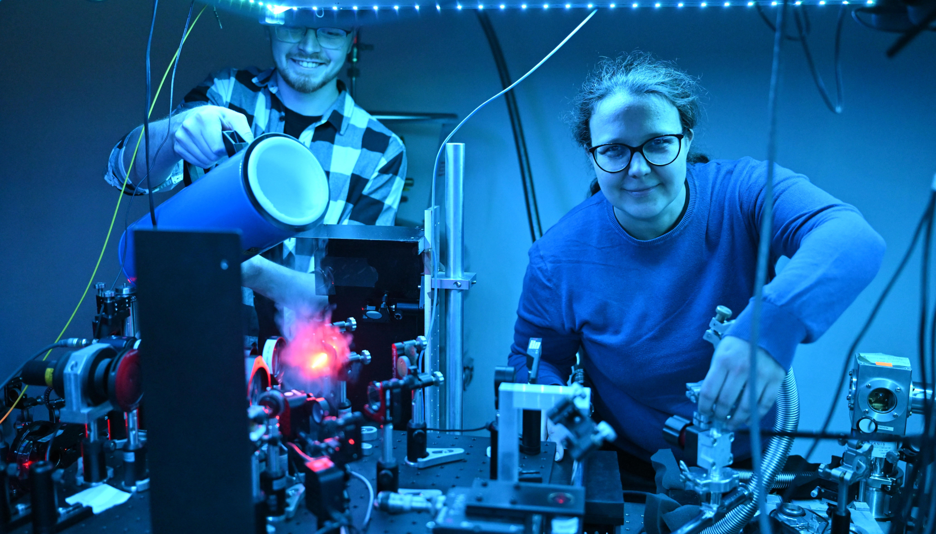
The very name may come as a surprise as a quantum dot does not have to have a round shape at all. It can just as well be produced in the form of a lens, pyramid, or cone. This is of considerable importance, as shape and size determine its properties, which are quite exceptional. That’s why scientific centres worldwide, including our research teams, are working on them.
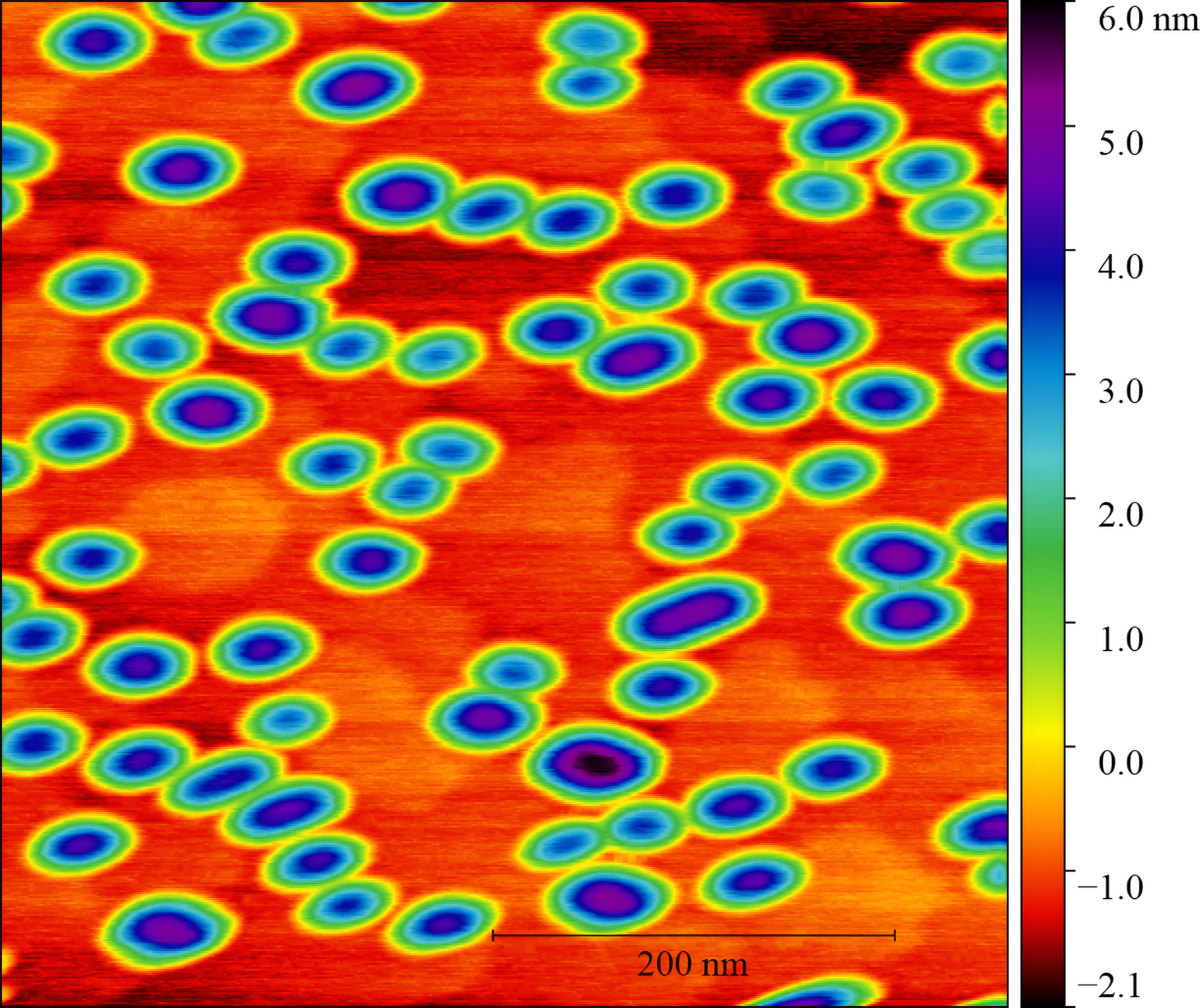 They are referred to as artificial atoms because of the similarity of their properties to natural atoms. A quantum dot – as explained by Anna Musiał, PhD, Eng. of the Department of Experimental Physics – is most easily imagined as a cubic box in which an electron is trapped – its motion is restricted in all three directions and the energies it can take depend on the size of the box. The smaller the box, the higher the energy of the electron.
Dr Anna Musiał is one of several researchers working at Wrocław University of Science and Technology who are involved daily in calculations and experiments connected with the research into the physics of quantum dots, the development of technologies using them, or the production of the dots themselves. This year, she has also become an ambassador for the quantum dot, popularising knowledge about it – as a researcher involved in the QuanTour project.
The initiative consists in a unique journey, entailing visits to 12 European countries, of a quantum dot enclosed in a special briefcase which is researched at each stop on its itinerary. The project also involves lectures, workshops, and meetings for people who want to learn more – about the dot itself but also about quantum mechanics and nanotechnology. We, too, would like to invite all of you who are interested in the subject to the talks, a tour of our labs, and a demonstration of single photon emission by a semiconductor quantum dot at Wrocław Tech during the “Quantum Dot Day” to be held on March 11, 2025.
A quantum dot is microscopic – on the order of billionths of a metre in size. The electrons enclosed within it are only in states with specific energies, and when producing such a dot, one can plan exactly what these energies will be.
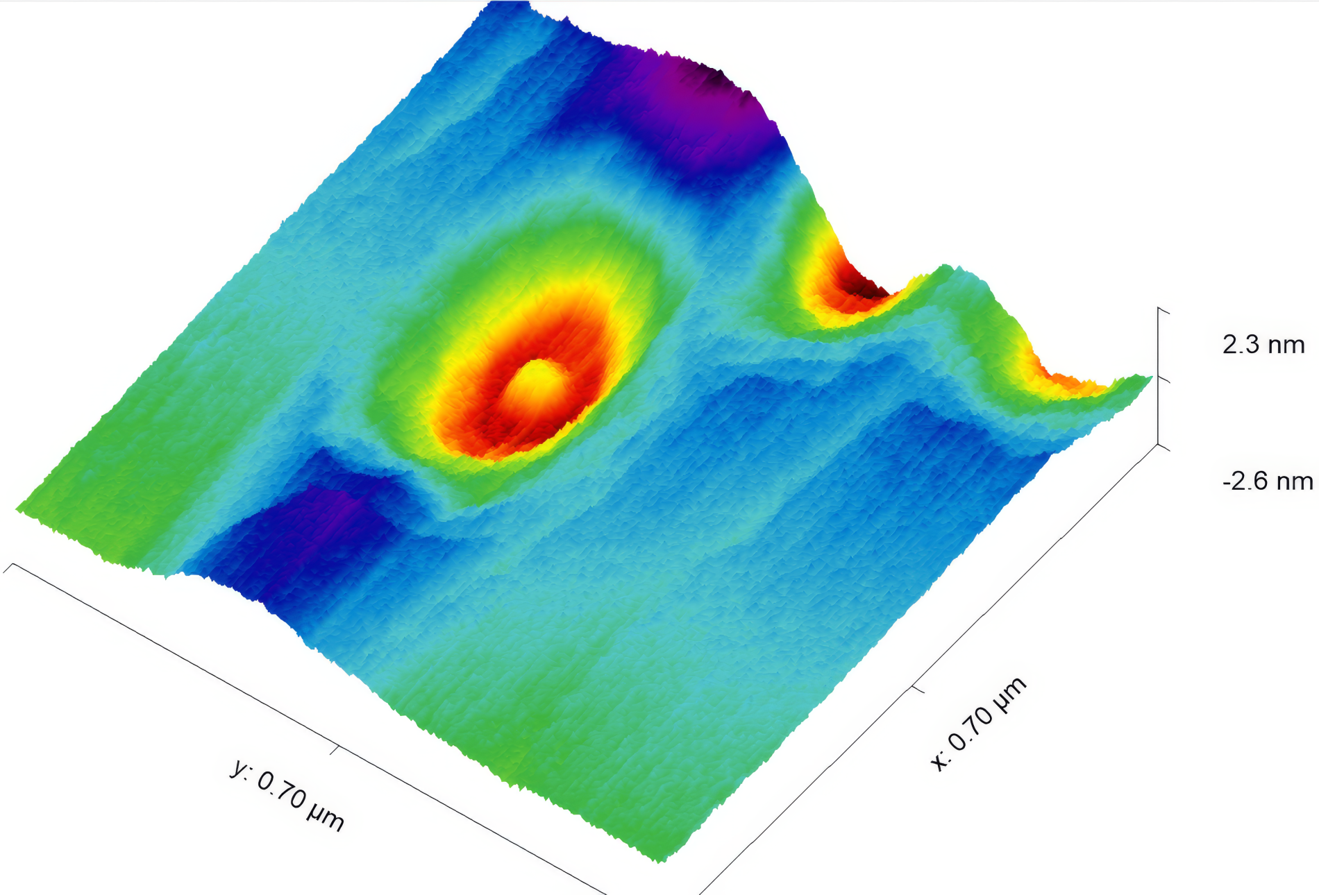 “If you compare a quantum dot to an ordinary atom, it’s easy to understand what its uniqueness is all about,” Dr Musiał stresses. “Each atom of a given type is identical and has specific properties that cannot be controlled. In an atom, an electron can only have strictly defined energies. We aren’t able to change that. Meanwhile, in the case of a quantum dot, we can design and manufacture it to have the arrangement of energy levels of our choice. This means that we can manipulate its shape, size, and structure to achieve the properties we need.”
And what properties are these? When the Nobel Committee announced the 2024 Nobel laureates in chemistry, its chairman, Swedish biochemist Johan Aqvist, placed five flasks filled with coloured luminescent liquids in front of him. Those were suspensions containing quantum dots. They glowed because quantum dots fluoresce, i.e. they absorb light and emit it in a single colour of our choice. This makes them excellent emitters, sources of light, among other properties.
We already use this daily – e.g. in computer screens and QLED TVs, which have layers of quantum dots used as a filter to increase colour intensity while maintaining high brightness levels. And these are just a fraction of the possible applications.
Scientists are already working on applications including the use of luminescent quantum dots in medicine, specifically in diagnostic imaging. There, they could serve as cell markers and help detect phenomena such as the spread of cancer or the migration of viruses. Research in this area is also underway at Wrocław University of Science and Technology – we’re partnering with doctors to check whether such dots introduced into the body will have a toxic effect on the environment and how they react to its parameters, such as pH*.
Medicine is one thing, but quite a few potential opportunities are also promised by the quantum dot in the area of engineering. For example, scientists are working towards using quantum dots to build miniature laboratories, so-called labs-on-chip.
Such laboratory systems with a quantum dot light source, detector, light guiding, and various components can fit on a small chip (which is important where every millimetre of space is priceless). At Wrocław Tech, related studies are being carried out by researchers including Associate Professor Marcin Syperek, PhD, DSc, Eng. and his group**, who intend to create a universal quantum photonic integrated circuit compatible with existing optical fibre infrastructure. It would combine multiple functionalities, such as on-demand emission of single photons and entangled photon pairs and their efficient detection. As a result, the invention would find applications in many areas of quantum communication, computing, and metrology, such as quantum cryptographic key distribution, remote quantum computing, or the synchronisation of atomic clocks through quantum entanglement.
“Another direction of research is the applications of quantum dots in the transmission of information, i.e. in telecommunications or quantum cryptography, which is also being researched by various teams at our department,” says Dr Musiał. “In this case, we force the quantum dot to emit photons in a particular state, such as single, indistinguishable photons or entangled photons. We can use them to perform tasks such as transmitting a cryptographic key securely. In this situation, the optical fibre is the transmission channel while the quantum dot is the emitter. If the key to decode the information is intercepted, we will know about it immediately. To explain it in the simplest terms: we will notice that someone takes one such photon away from us. And even if someone were to try to just measure it, we will detect that too, because its condition will change, and we will spot that right away.
The researcher adds that for such a solution to become useful (i.e. to be applied also outside laboratories), it’s necessary to take steps including modifying the properties of quantum dots so that they produce the signal from the dot as frequently as possible (i.e. emit photons at the highest possible frequency), developing very sensitive detectors that will be able to capture single photons, miniaturising the entire system, and permanently connecting the emitter with the optical fibre***. Assuming these goals is resulting in the months-long (and often international) work in the team headed by Prof. Grzegorz Sęk****, including Dr Musiał’s research projects*****.
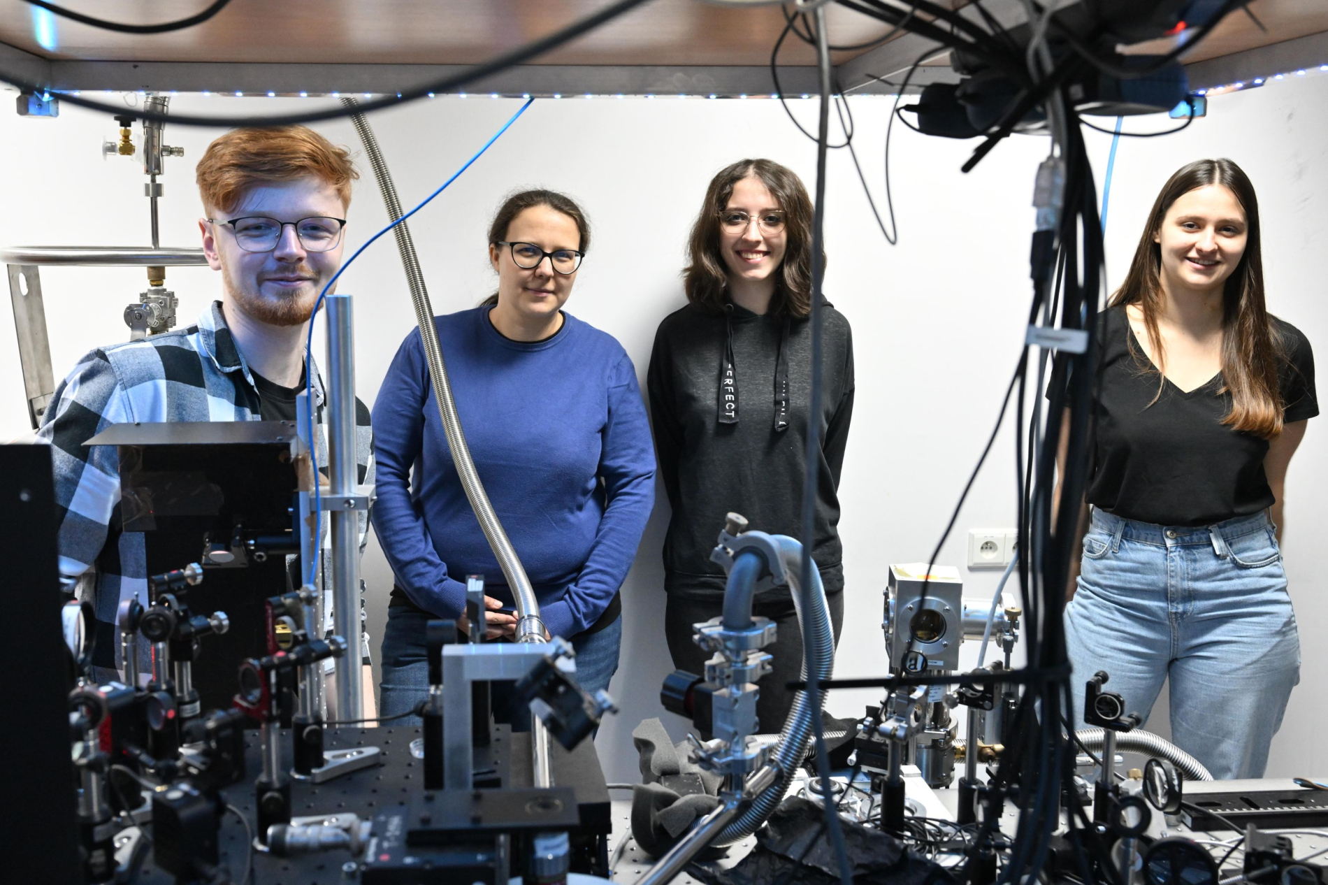
“We want to use quantum dots to transmit information over long distances. As far as optical fibres go, the smallest losses occur in the so-called telecommunications windows – at wavelengths of 1,550 and 1,310 nanometres,” says Dr Musiał. “Bearing this in mind, we’re aiming to develop dots that emit waves in this range in collaboration with foreign partners. Such wavelengths may also be attractive in terms of transmitting information in the atmosphere, to the satellite and back.
At the same time, researchers are developing methods for the very production of quantum dots, as how they are made and what materials are used impact their properties. Just manipulating the size changes their behaviour and characteristics, i.e. their optical, magnetic, electrical, and chemical properties. The properties are also influenced by the shape of the dot. It all means that the possibilities are practically endless.
As Dr Musiał explains, dot generation technologies can be divided into two groups: “bottom up”, i.e. building from atoms from scratch, and “top down”, i.e. the approach that consists in stripping away excess material to eventually create a dot.
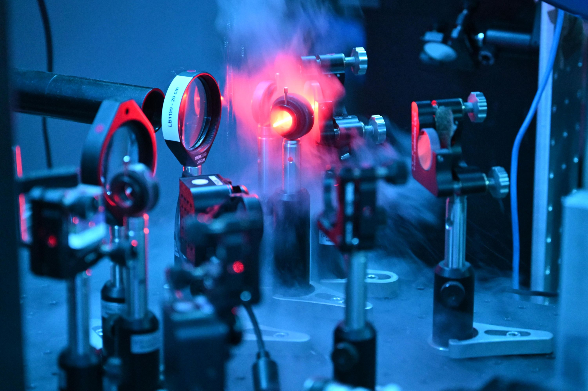 “The ones we deal with in our team are created using so-called epitaxial methods, i.e. the bottom-up approach,” says Dr Musiał. “These methods involve the selected substrate material being heated in a reactor under vacuum conditions and layer upon layer of other materials being applied. We’re currently researching structures based on indium phosphide and gallium arsenide, and recently also gallium antimonide, among other ones. The latter are produced by our consortium partners in a laboratory in Finland, and these are the dots we are working on as a large international team with a view to developing telecommunications solutions*****.
Dots can also be produced electrostatically, by controlling an electric field in such a way as to trap electrons, or by physico-chemical synthesis. The latter is what the team led by Prof. Artur Podhorodecki, also from the Department of Experimental Physics, from which the start-up QNA Technology spun off. The group is working on synthesising, functionalising, and studying colloidal quantum dots with applications in optoelectronics and photovoltaic modules in mind. It’s also developing technologies using dot-based nanomaterials for displays, LED lighting, photonics, and printed optoelectronics.
“There are dozens of teams in Europe alone that are involved in quantum emitter-related research daily, and several of them are focusing on quantum dot-based solutions. It’s therefore a very current subject with huge development potential,” emphasises Dr Musiał. “It’s a bit of a race to see who will be the first to develop new and better solutions based on quantum dots with advantages over other ways of generating photons that are attractive from an application point of view.
In addition to the potential applications mentioned earlier, researchers also see the future of quantum dots in the development of so-called quantum information processing (i.e. quantum computing, because certain computational tasks can be performed more efficiently thanks to algorithms that take advantage of the quantum nature of the circuits), random number generators, metrology, imaging, flexible (elastic) electronics, very small sensors, and thin solar cells.
* Also involving the project “Synthesis of Inorganic Nanocrystals Doped by Lanthanide Ions for Bio-Medical Applications (SINDBAd)” (2011-2014).
** Research in the field of integrated photonic systems is being carried out by Dr Marcin Syperek, Prof. of the university, and his group. These include the HORIZON2020 (EU) 2023-2027 projects: Quantum photonic integrated circuits at 1550 nm (project leader - Prof. Syperek), Sonata Bis (NCN) 2024-2027: Integrated quantum photonics on a hybrid InP/SiO2 platform (project leader - Dr Eng. Paweł Mrowiński) or Sonata (NCN) 2021-2024: Heterogeneous waveguide structures on the Si platform with InAs/InP quantum dots emitting in the 1.55 μm spectral range for application in scalable photonic circuits (project leader - Dr Eng. Paweł Mrowiński).
***Interesting research in this area is being carried out, among others, by Kinga Zolnacz, PhD, Eng. from W11’s Department of Optics and Photonics. Her method involves locating the structure on the surface of the sample using an interferometric method and then permanently connecting an optical fibre to the quantum emitter in the photonic structure. You can read about the details in the article entitled “Method for direct coupling of a semiconductor quantum dot to an optical fibre for single-photon source applications”. The method was used by the researcher to produce a fibre-optic source with which quantum transmission of a cryptographic key was demonstrated.
**** Prof. Sęk is currently heading two quantum dot-related projects. The first is “Quantum Dot coupling engineering (and dynamic spin decoupling/deep nuclei cooling): 2-dimensional cluster state generation for quantum information processing (QCEED)”, funded under the Horizon Europe Pathfinder programme. The research focuses on quantum dots emitting in the telecom infrared range for use as quantum emitters in sources of non-classical light states for cryptography and quantum communication in optical fibre networks. The second project, named “Optical, structural and electronic properties of III-V quantum dots on silicon”, funded by the National Centre for Science under the OPUS programme, is related to quantum dots integrated into a silicon platform.
***** It concerns the project named “Fibre-Coupled GaSb Quantum Dot Tuneable Single-Photon Sources for Field Deployed Quantum Key Distribution – FiGAnti”, funded under the QuantERA II programme.
Lucyna Róg
Our site uses cookies. By continuing to browse the site you agree to our use of cookies in accordance with current browser settings. You can change at any time.